Optics
Vision & Sensors
V&S
Recent breakthroughs in sensor technologies have shown great promise in SWIR moving into the machine vision mainstream.
By Jeremy Govier
Advancements in
Short Wave Infrared Sensors
Imaging using short wave infrared (SWIR) radiation has long offered interesting properties for industrial machine vision but has been slow to be adopted. SWIR offers many useful properties that can make things that are invisible under white light become visible, as well as making opaque objects under white light transparent. This can allow machine vision lenses to see into objects they otherwise could not, increasing contrast between objects that otherwise look very similar. But despite these advantages, the adoption of SWIR has been very slow.
Recent breakthroughs in sensor technologies have shown, however, great promise in SWIR moving into the mainstream of machine vision. These new breakthroughs have resulted in new imaging sensors covering visible and SWIR wavelengths with a high quantum efficiency (QE), which describes how efficiently incident light is converted to electric signals. High sensitivity to both visible and SWIR wavelengths is something that has garnered a lot of interest and discussion already, but the other attributes of the sensor are also very interesting and important for their adoption in industrial machine vision and inspection.
What Makes These New Sensors Special?
In addition to a good QE over wavelengths from 0.4 to 1.7µm, these new sensors offer smaller (5µm) pixels, low noise, and high pixel quality. These qualities are all things expected in the visible spectrum for an industrial CMOS sensor but are rare for SWIR systems. This means that SWIR sensors are moving closer to the quality demanded by the machine vision and inspection industry.
Smaller pixels allow for more pixels over a given sensor size, which offers several important benefits. First being reducing the cost of the sensor, as smaller sensor sizes means more sensor can be fabricated per semiconductor wafer. This also affects the cost of the optics. As the sensor size goes down, the focal length of the lens for any given angular field of view will also go down, which will reduce the size and cost of the optics required. The smaller pixels lead to physically smaller and lighter optics, allowing for easier integration into industrial environments.
Low noise is a key parameter for machine vision because noise can result in measurement errors, slower decisions, and false decisions. Reducing noise at the sensor can also speed up inspections as less noise reducing averaging of the data needs to be done.
High pixel quality or a lack of pixel defects has long been a standard requirement for industrial sensors in the visible but has been a significant problem in InGaAs sensors for the SWIR in the past. Low pixel quality results in the need to do further image processing to find and ignore data from bad pixels, slowing processing and resulting in less useful information.
The good quantum efficiency is an important requirement for an industrial machine vision sensor. High QE means that less photons are needed to generate a strong electrical signal. The better the QE, the shorter the exposure that is needed, which means in an industrial application fast-moving parts can move past the camera with minimal motion blur. Less lighting is needed or smaller aperture lenses can be used when the QE is high. For SWIR imaging, having a high QE is especially important.
The specific attribute of having high QE in the visible, while unique for a SWIR sensor, is not something that is as exciting for machine vision. So, despite it being the property that is being talked about the most, it is likely not nearly as important to the adoption of the new sensors as the many other positive attributes mentioned above.
SWIR Imaging Applications
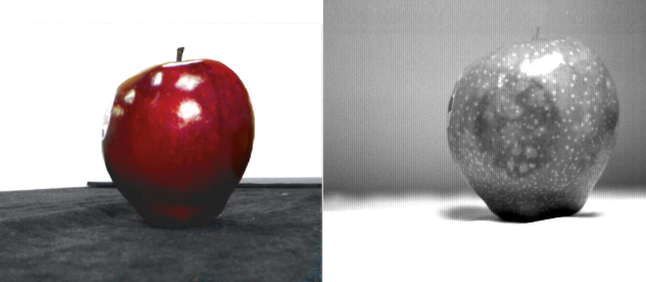
SWIR light interacts with many materials differently than visible light. Some objects will be transparent or semitransparent in SWIR but opaque in visible. Some plastics can be seen though in SWIR but are opaque in the visible, allowing for the inspection of the contents of an opaque white bottle (Figure 1). Similarly, silicon substrates become transparent in the SWIR and you can inspect components that would otherwise be obscured in visible light. Some objects absorb SWIR light that otherwise reflect visible wavelengths, making otherwise white objects appear dark in the SWIR. This can be used to identify and separate materials that would otherwise appear identical in the visible. SWIR can penetrate the surface of a lot of organic material allowing for imaging things just below the surface, such as bruising of produce (Figure 2).

Figure 1: A SWIR imaging system can image through this opaque white bottle to reveal the profile of the hidden substance inside the bottle.

Figure 2: SWIR wavelengths can reveal bruising in produce that is invisible when inspecting the produce using visible wavelengths.
All of these phenomena that take advantage of the ways SWIR interacts with material differently than visible wavelengths can only be seen if the SWIR light is captured by the sensor. If the sensor also sees a white light image in addition to the SWIR, the visible light information will cloud over the information from the SWIR, losing contrast or obscuring it completely. To avoid this, either only SWIR light needs to be used in the illumination, or filtering needs to occur to block the visible light. Many applications will only need the SWIR information so just illuminating with SWIR or using a filter that passes only the SWIR will suffice.
There are some applications that require alternating information from visible to SWIR wavelengths. For example, in the earlier produce inspection example, the SWIR only would be used to look for bruising, but the visible light could be used for looking for produce color. For this application, alternating illumination could be used, but this would require that the object is only being illuminated by light that can be controlled and not additional ambient sources. For applications where the illumination is not entirely controlled, filtering will be necessary. Alternating filters can be difficult and expensive to automate, so using multiple cameras can often be simpler and cheaper, especially for the case where one camera is only looking at the visible light. A visible light camera and lens will be significantly cheaper than the SWIR camera and lens for a comparable resolution.
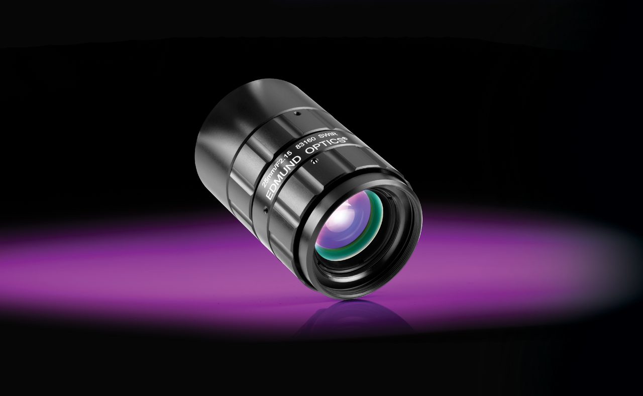
For imaging both SWIR and visible wavelengths there is another consideration: chromatic aberration. Even in simple visible lenses there exists a phenomenon called chromatic aberration that reduces performance. This comes about from a physical property of the glass used in the lenses of the imaging assembly called dispersion, which is a change in the bending power of a glass with respect to wavelength. This dispersion causes chromatic aberration in which different wavelengths will be focused differently by the lens. Chromatic aberration can be minimized in the lens design by carefully balancing what materials with different dispersion values are used to affect where each wavelength is focused. The vast majority of off-the-shelf camera lenses are color corrected for the visible light. There are a smaller number of lenses optimized for color correction over just the SWIR. These lenses tend to be several times more expensive than a comparable visible-designed lens (Figure 3). Many things drive this higher cost but primarily it is the complexity of correcting the chromatic aberration in the SWIR. Correcting chromatic aberration in the SWIR is more difficult because optical glasses act differently at these wavelengths and do not have the kinds of dispersions that are ideal for balancing the chromatic aberration. Many lens elements are used, making the designs more complicated and expensive because of the less ideal choices of dispersions available for correcting the chromatic aberration. When being used monochromatically or over a relatively small band of wavelengths, a lens not designed to be color corrected for the SWIR can still preform adequately. Because of this, a lens designed for visible light can be used in the SWIR when using either a narrow filter of narrow band illumination, such as LEDs.

Figure 3: It is possible to make imaging lenses corrected for chromatic aberrations spanning both the visible and SWIR spectra, but this is more complicated and costly than lenses corrected for a smaller wavelength range.
However, if you want to use both visible and SWIR light, a very complex amount of color correction is needed. This is possible and lenses do exist on the market that perform excellently. However, it is very complex and thus expensive. The cost of a color corrected lens working in visible through SWIR is several times more expensive than a lens color corrected for just SWIR.
Applications requiring the use of both visible and SWIR can use a single new SWIR sensor and a single lens color-corrected for visible through SWIR wavelengths along with either alternating illumination between the two or a moving filter option. Alternatively, a new SWIR sensor could be used with a SWIR designed lens and a SWIR-pass filter, and a second visible only camera with a standard visible lens could be used to result in significant cost savings without requiring moving parts or alternating light sources.
The new visible-SWIR sensors entering the market offer significant advantages for SWIR industrial machine vision, such as small pixels, good QE, low pixel defects, and low noise, even if this particular market will not be taking advantage of the visible light sensitivity.
All Images Source: Edmund Optics
Jeremy Govier, principal engineer at Edmund Optics. For more information, email JGovier@edmundoptics.com.
Scroll Down
Scroll Down

