PIXEL
The Shrinking
Test & INspection
What motivates smaller pixels? It’s mainly cost, which is directly tied to image sensor size.
By Perry West
How small can pixels on an image sensor become? We probably don’t know the answer except that they might become very, very small. Semiconductor processing is able to produce features as small as 5 nanometers. And while this extremely small size may not work for pixels on an image sensor, it shows we are not anywhere near the size limit.
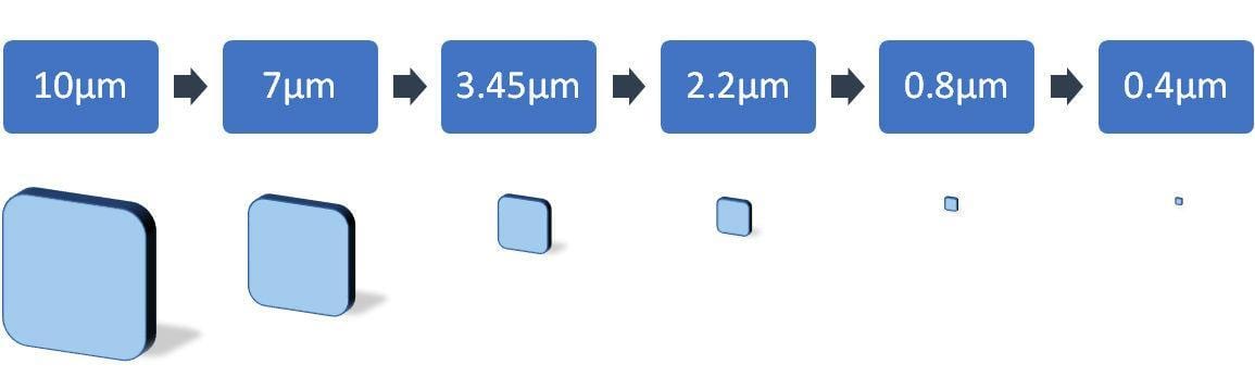
In the early days of machine vision, pixels were 17µm. A bit later, with the appearance of VGA resolution sensors in a 2/3 inch format, they became 13µm. From that point on smaller sensors and higher resolution have pushed pixel size downward to 10µm, 7µm, 3.45µ, 2.2µm, and even to 0.8µm today. At least one image sensor company has a roadmap to 0.4µm pixel size.
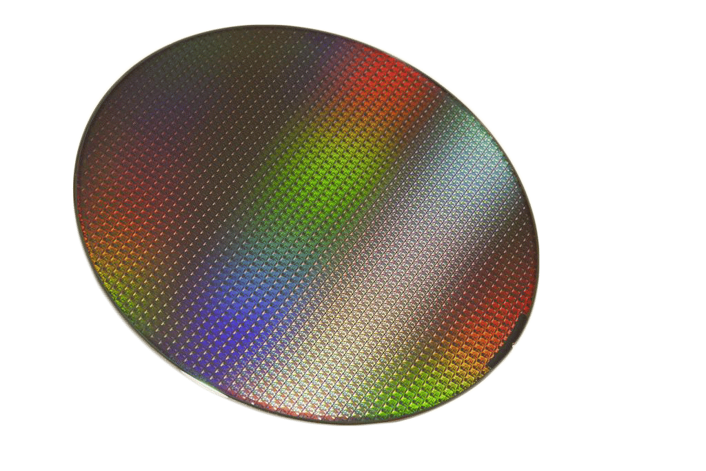
Figure 2 - Silicon Wafer
Photo by Rob Bulmahn, Creative Commons License
Figure 1 - The Shrinking Pixel
What motivates smaller pixels? It’s mainly cost, which is directly tied to image sensor size.
A processed 300mm wafer costs between $4,000 and $14,000 depending mainly on the “node” or how small the features can be. The node ranges from 45nm down to 5nm with smaller node processes costing more. It also depends on the number of process steps needed to fabricate the wafer. Also, wafers are processed in lots of at least 20 wafers.
To gain economy, it becomes necessary to increase the number of image sensors per wafer. The easiest way is to make the image sensors smaller.
Smaller image sensors conflict with the demand for ever higher image resolutions – the number or rows and columns of pixels – or megapixels.
How does a company create both smaller image sensors and maintain or increase image resolution? Only by making the pixels smaller.
What is the downside of small pixels? The first drawback is noise. A dominant form of noise in image sensing is photon shot noise – an effect of quantum physics. Photon shot noise is proportional to the square root of the number of photo-generated electrons. The more photo generated electrons, the lower photon shot noise is as a percentage of the signal.
Larger pixels have a larger area to capture photons and a larger capacity to store photo generated electrons called the full well capacity. Because smaller pixels have a corresponding smaller full well capacity, their photon shot noise will be proportionally larger.
Another drawback to small pixels is having optics that will match the pixel size. There’s a formula for diffraction, the fundamental limitation of lens resolution:
R = 1.22 λ f#
Where λ is the wavelength of light and f# is the f-number of a lens.
For λ=555nm, green light where the human eye is most sensitive, and f-number = 1, a very wide lens, the resolution limit is 0.68µm. Before you conclude that optics can resolve detail commensurate with the small pixel, realize this is a theoretical limit that does not take into account other lens aberrations. Also, lenses with low f-numbers are more difficult to design and more expensive to manufacture.
The design of a diffraction limited lens with a wide aperture is possible. It is a very complex lens with exceptionally tight manufacturing tolerance, and excludes much flexibility such as the ability to focus to different working distances. As such, it would become a very expensive custom lens.
Figure 4 - MTF of Image Sensor
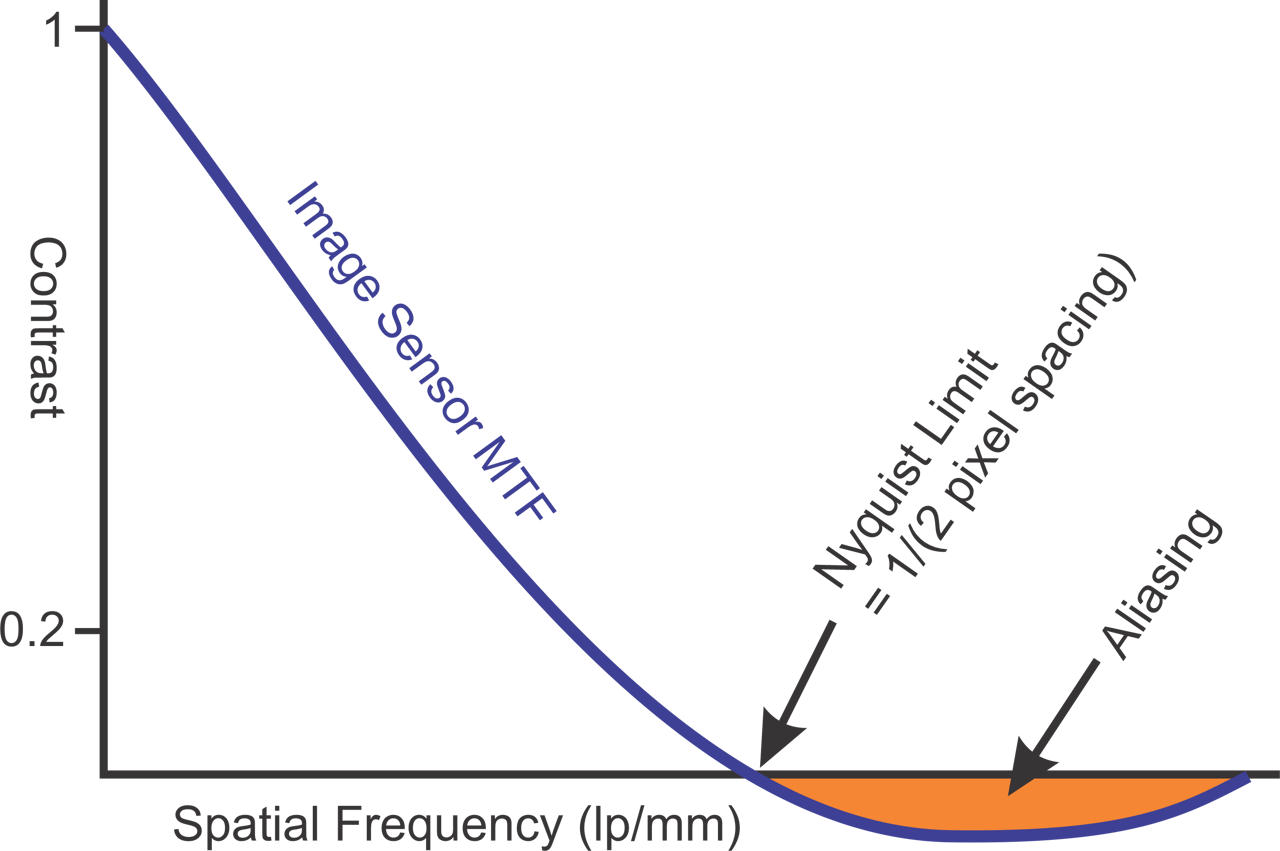
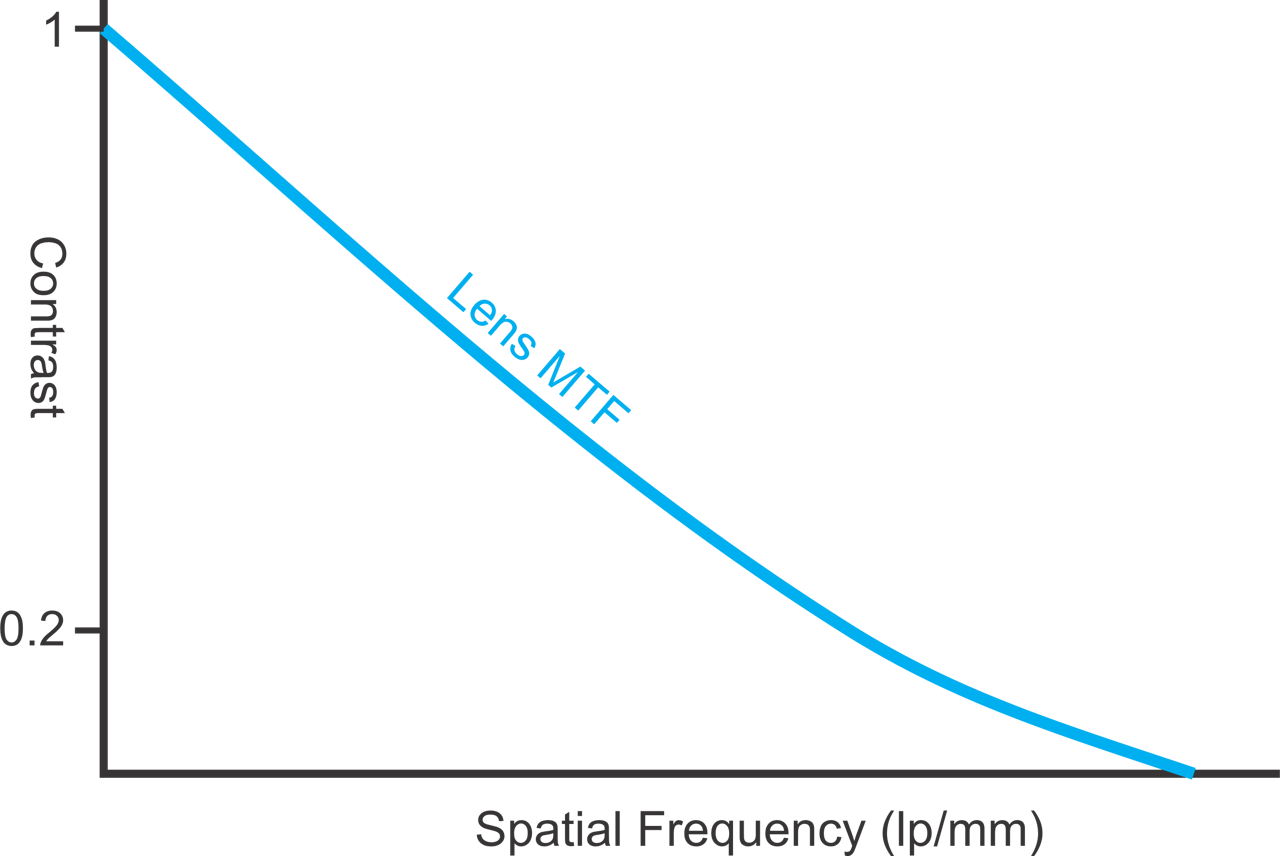
Figure 3 - Lens MTF
There are some upsides to small pixels. One will become apparent when we look deeper into resolution. Another may emerge when we look into how the small pixels can be used together in groups.
Perhaps you know about modulation transfer function (MTF) for a lens. This shows the contrast a lens can produce as a function of detail called spatial frequency. To understand spatial frequency, consider that you have a pair of lines, one white and one black, both equal in width. Now ask how many of these line pairs will fit side by side in a millimeter. As the lines become narrower, more pairs will fit into one millimeter. The width of the lines represents the detail the lens can resolve optically.
Notice, as the spatial frequency increases, there comes a point where the lens cannot produce any contrast; it cannot resolve this detail. For vision system work, 20% contrast is often used as a target limitation on lens resolution or the spatial frequency.
Many people do not realize an image sensor also has a MTF. And it’s different from that of a lens. The contrast starts out at 100% and gradually declines to zero. Then something strange happens; it continues, but it’s negative. What is happening in this negative region is that the information is affected by aliasing – the difference between the spatial frequency, the spacing of the light and dark lines, and the pixel spacing. The point where contrast reaches zero is the Nyquist limit and is two times the pixel size.
Figure 6 - Matched MTF Curves for Lens and Image Sensor
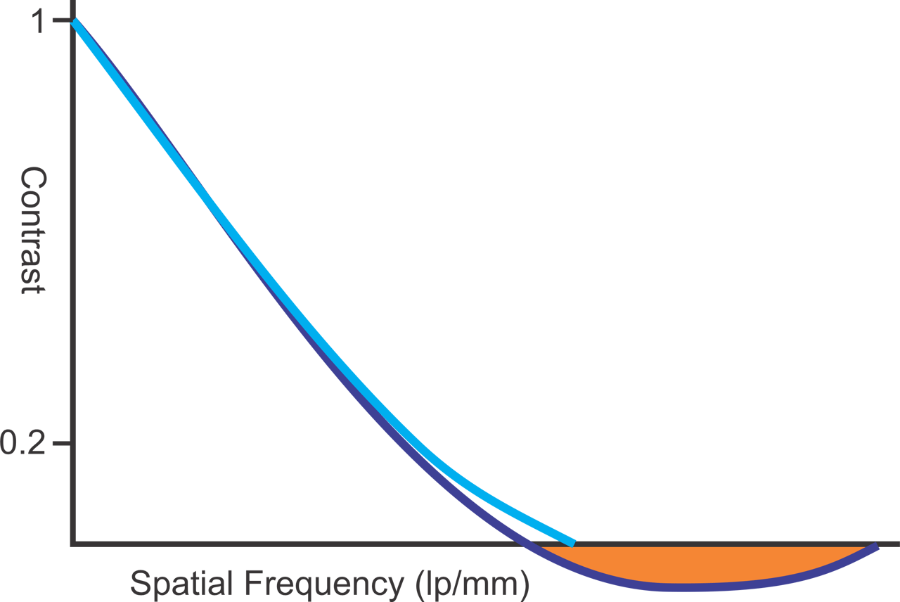
Figure 5 - MTF of Image Sensor and High Resolution Lens
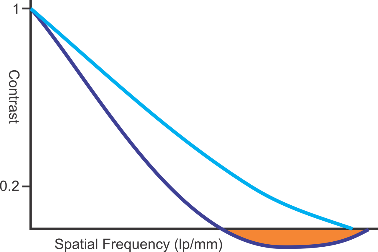
It is common for people to pick a lens with optical resolution well above the Nyquist limit. This means that the corrupted data from the image sensor will deliver an image where edge profiles are corrupted. Systems making precision measurements may have their accuracy limited by this corruption.
One possible solution is to pick a lens with an optical resolution limit right around the Nyquist limit. This prevents image data corruption. The combined imaging MTF is just the two MTF curves multiplied together. At a point where the lens gives 20% contrast and the image sensor gives 20% contrast, the contrast in the image will only be 4%, possibly too low for many applications.
Figure 8 - Bayer Filter Pattern on an Image Sensor
Figure 7 - Lens Limited MTF
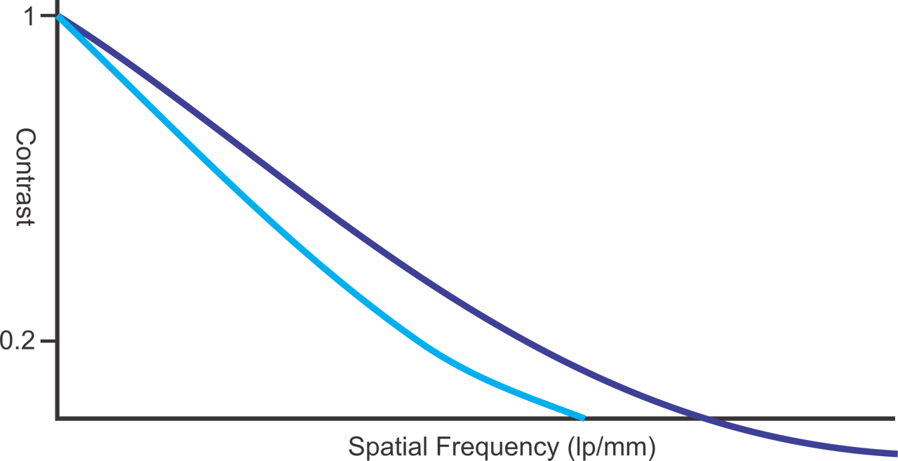
When the Nyquist limit for the image sensor exceeds the lens’ optical resolution, then aliasing does not corrupt the image and the combined contrast can be higher than that of a matched sensor and lens. We should not forget, though, that this comes at the expense of a somewhat noisier image and more image data to transmit and process.
Using groups of small pixels rather than individual pixels may give improved imaging capabilities. For example, the very common Bayer filter pattern where each pixel has a color filter over it and the other two colors for three-color imaging are derived by interpolating nearest neighbors gives rise to artifacts such as purple fringing.
Figure 10 - 4x4 Bayer Filter Pattern

Figure 9 - Enlargement Showing Purple Fringing
Photo by Hayden Kirchner, Creative Commons License
Suppose, instead of the Bayer pattern on adjacent pixels, a four-by-four array of small neighboring pixels had color filters and the image sensor could bin, that is, combine, the signals from pixels with the same color filters. This would virtually eliminate the purple fringe and also, through binning, reduce the effect of photon shot noise.
The idea for three color filters, red, green, and blue, is to reproduce most of the color gamut visible to humans that have three different color sensors, cones, on the retina. For a different model, look at the mantis shrimp. Its eyes have twelve different cones enabling it to see beyond the visible spectrum into ultraviolet and infrared. Not only can the mantis shrimp see wavelengths not visible to humans, it has the potential to differentiate colors better than humans. The mantis shrimp is also able to sense the polarization of light.
Figure 12 - Multi-Spectral and Polarization Filter Pattern

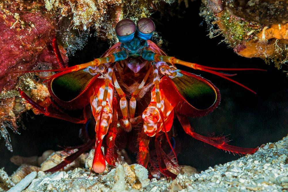
Figure 11 - Mantis Shrimp
Photo by Francois Libert, Creative Commons License
Returning to the four-by-four group of small pixels, it would be possible to use a range of color filters to extend the color gamut and discrimination and also to sense polarization of light. This arrangement would introduce the ability to perform multi-spectral or hyperspectral imaging into 2D image sensors.
In conclusion, pixels will shrink driven by cost pressures of consumer devices where the engineer cost to mitigate their limitation is amortized over huge volumes. For most technical imaging, the pixel size will likely stay around 3µm where noise is more manageable and lenses more practical to design and manufacture. However, groups of small pixels used in unique ways may also open new imaging opportunities.
Opening Video Background Source: luza studios/Creatas Video via Getty Images.
Source for images not otherwise specified: Automated Vision Systems Inc.
Perry C. West is president of Automated Vision Systems Inc. (San Jose, CA). For more information, call (408) 267-1746, e-mail perry@autovis.com or visit www.autovis.com.
February 2022 | Volume 61 | Number 2